论文总字数:18364字
基于matlab的sigma-delta调制器的设计
陈凯玲
,China
Abstract:Sigma Delta ADC (Analog to Digital Converter) is mainly composed of two parts: Sigma Delta modulator and digital filter. Compared with other types of ADCs, its advantages are higher conversion accuracy and lower power consumption. Among them, Sigma Delta Modulator has insensitivity to various non-ideal factors in process production, and it has lower requirements for analog circuit design, so it has been widely used in audio signal processing. In addition, the use of techniques such as oversampling and noise compression enables the Sigma-delta ADC to achieve high-precision analog-to-digital conversion.
Scholars comparing Sigma-delta ADCs with conventional analog-to-digital converters has found that sigma-delta ADCs not only have lower requirements for analog circuit performance and device matching, but are also easier to implement on-chip integration with other digital circuits. Therefore, the sigma-delta ADC has also been widely used along with the rapid development of the system-on-chip (SOC). This paper starts from the working principle of the sigma-delta modulator and discusses in detail the impact of non-ideal factors such as clock jitter, switching nonlinear resistance, and switching thermal noise on the performance of the modulator. Then, based on the above non-ideal factors, this paper deduces the time domain mathematical model of the modulator's performance. Based on this model, using simulink under MATLAB software, non-ideal construction of first-order and second-order sigma-delta modulators is performed. Using the method of simulation analysis, the module obtains the influence of non-ideal factors on the SNR of the modulator. Finally, this paper proposes the idea of global optimization design, that is, how to design the modulator circuit parameters in order to achieve the best performance of the modulator.
Key words:Sigma Delta Modulator; Precision; Power Consumption; Oversampling Technology; Noise Shaping Technology
第一章 绪论 5
1.1 研究背景与意义 5
1.2 国内外研究现状 5
1.3本文主要研究内容和结构 8
第二章 sigma-delta的基本原理 9
2.1奈奎斯特ADC 9
2.1.1采样过程原理 9
2.1.2量化过程原理 10
2.1.3 奈奎斯特 ADC 的主要类型介绍 11
2.2 过采样 12
2.3 噪音整形 12
2.4 ADC的性能指标 13
2.5本章小结 13
第三章 一阶Sigma Delta调制器设计 14
3.1一阶Sigma Delta 调制器时域分析 14
3.2一阶Sigma Delta 调制器频域分析 14
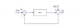
3.3一阶Sigma Delta 调制器系统模型图及仿真分析 15
3.3.1 一阶Sigma Delta 调制器系统模型图 15
3.3.2 一阶Sigma Delta 调制器的仿真分析 15
3.4 总结 17
第四章 二阶Sigma Delta调制器设计 18
4.1二阶Sigma Delta调制器频域分析 18
4.2二阶Sigma Delta 调制器系统模型图及仿真分析 18
4.2.1 二阶Sigma Delta 调制器系统模型图 18
4.2.2二阶Sigma Delta 调制器的仿真分析 19
4.3 总结 29
第五章 总结与展望 30
参考文献 31
致谢 32
绪论
研究背景与意义
21世纪以后,集成电路产业取得了飞快的进步,其器件尺寸不断缩小、速度不断提升、集成度也越来越高。这一硬件的进步为电路设计所遵循的低功耗、高速、低成本、高密度的要求提供了实现的基础[1]。数字电路因其在噪声干扰、稳定性、集成度、经济成本等方面都比模拟电路具有显著的优势,还方便数字计算机处理,越来越受到电路设计的青睐。此外,得益于计算机硬件的不断优化,软件技术的不断创新,数字信号处理技术也愈发成熟,数字技术的发展具有广阔前景。目前,数字技术已经渗透到社会各个领域,我们周边各种科技产品都离不开它的身影,比如手机、电视、地铁等等,或许说只要有电、有控制的地方,就离不开数字技术的支持[2,3]。虽然数字电路、数字技术都有极大的优势,但任何一个系统跟自然界在信息交互的过程中,自然界只能传递随时间和空间连续变化的模拟信号。所以,为了实现信息的联通,必须通过转换技术将自然界的模拟信号转换成数字信号,以便于系统后期通过各种技术手段对其加工处理[4,5]。能够将模拟信号转换为数字信号所依赖的设备就是模数转换器(ADC)。经过众多科研人员的日夜攻关,数字技术发展迅猛,不断带来新的惊喜,与此同时,制造业实力的提升使得超大规模集成电路制造成为可能。伴随着数字产品走进千家万户,模数转换器的应用范围越来越广,相应的,越高端的科技产品对模数转换器的性能要求也越来越高,主要体现在精度和速度两个方面。模数转换器(ADC)有不同的分类标准,以采样频率为例,可分为 Nyquist 采样ADC 和过采样ADC。 Nyquist又因结构不同分为低速、中速、高速三种类型。Nyquist 采样ADC相较于过采样 ADC,在制造工艺、模拟电路方面都需要较高的性能要求。这是因为过采样 ADC采用了过采样、噪声压缩等技术所以在模拟电路面适配性强,对性能要求不够严苛。这样的特点使得过采样 ADC在高精度应用场合有着广阔的前景。相比于Nyquist 采样ADC,过采样 ADC因其更能与数字系统兼容,所以在速度、精度、功耗、集成度、成本这几大方面都具有显著优势,也更贴合集成电路 SOC以后的发展走向。本文通过上述比较,决定以过采样 ADC作为研究对象,从各个方面系统地对其展开研究。
国内外研究现状
Cutler在对Δ调制以及ΣΔ调制的研究中,提出了一个基本的研究思想,即依靠反馈来提高粗位量化器的有效分辩率,事实证明,这一做法效果显著。Cutler在其1954年提出的专利中详细描述了这一概念,并且在1960年获得专利批准。他在专利中提出,其为提高有效分辨率是通过在原系统的基础上,从输入信号中加上或减去量化噪声,这一噪声是位于前馈通路上的低分辩率粗位量化器所产生的[6,7]。在此之后,Spang 和 Schultheiss 继续对 Cutler 的研究进行分析,对系统Cutler做了优化,提出了多个改进措施和方法。最突出的是,Spang和Schultheiss提出将有限冲击响应滤波器(FIR)添加在前馈通路上,这样一来系统就能够对下一个量化误差进行预测和修正[8,9]。后来,学术界将Spang改进过的系统称为误差反馈编码器(Error Feedback Coder)。
Jager 等人于1952 年提出Δ调制器,这种调制器将一个量化器放置在前馈通路上,将一个环路滤波器放置在反馈通路上。其中,量化器通常是一位的,而环路滤波器有多种选择,具体视系统要求而定,系统要求不高时可以由一个积分器充当。Δ调制器也属于误差反馈编码器,所以基本思想是一致的。系统在运作中的信号和量化噪声都会被反馈、滤波,之后与输入信号相减。对于输出信号来讲,它包含了输入信号和量化噪声的微分量,在接收端通过一个积分器起到信号存储作用。Δ调制器在充当ADC 时,并不能取得良好的效果,往往存在严重的问题。主要因为以下两点:一是误差反馈系统需要在反馈端有精准的相减电路,这一要求通过电路设计来实现难度极大。二是Δ调制器因在接收端需要积分器作为信号存储,对信号的低频段有抑制作用,而且因为信号频率增加使得系统的动态范围下降。
剩余内容已隐藏,请支付后下载全文,论文总字数:18364字
相关图片展示: